
Plasma-enhanced chemical vapor deposition (PECVD)
Coatings in the semiconductor industry and photovoltaics
Plasma-enhanced chemical vapor deposition, often simply referred to as PECVD, is a cyclic CVD process. This process is characterized by its special ability to deposit surface-conforming coatings with high-level precision in their thickness.
- This enables coatings to be applied at low temperatures
- Suitable for temperature-sensitive substrates – such as plastic
- Complex component coating possible
Find out more about this reliable and precise technique in thin film technology.
How It All Works
WHAT IS BEHIND PLASMA-ENHANCED CHEMICAL VAPOR DEPOSITION?
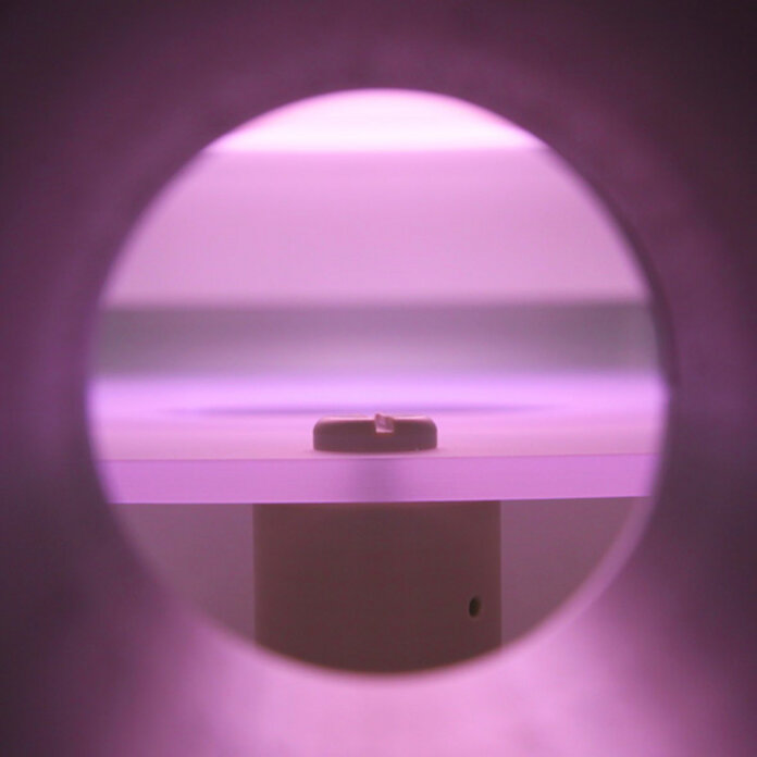
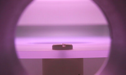
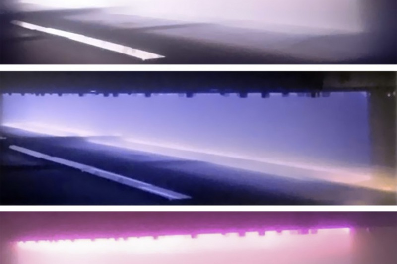
In plasma-enhanced chemical vapor deposition – or PECVD for short – plasma is used to support a chemical reaction. The advantage of this method is that lower temperatures between 200 °C and 500 °C can be used. This is particularly gentle on the substrate to which the coating is being applied.
With the direct plasma method, the plasma can be ignited directly next to the substrate. However, this process harbors the risk of damaging sensitive substrate materials – such as semiconductor wafers. This is why the remote plasma method is often used, in which the plasma is separated in spatial terms from the carrier material – a barrier protects the substrate from damage, and also enables the selective excitation of individual components of the process gas mixture. With this process, however, it is important to ensure that the chemical reaction only takes place when the activated particles reach the surface of the substrate.
These “low-temperature CVD” processes are often used when the substrate – e.g. plastic film – cannot withstand high temperatures. The semiconductor industry also relies on this method to avoid any structural changes in the semiconductor. PECVD technology can also be used to deposit a wide range of materials – such as amorphous silicon, silicon nitride or silicon oxide for microelectronics. FHR’s PECVD systems are customized and specially adapted to the respective process requirements. PECVD compartments are also frequently used to extend the technological range of sputtering systems. In any case, FHR delivers an impressive performance with its competitive prices and outstanding system quality.
Plasma-enhanced chemical vapor deposition (PECVD) offers numerous advantages:
- Surface conformity: PECVD enables the deposition of coatings that closely match the substrate’s topology, which is particularly important for structured or uneven surfaces.
- Low processing temperatures: By using plasma, PECVD can be performed at lower temperatures than with traditional CVD processes, which is particularly advantageous for temperature-sensitive substrates.
- Versatility: PECVD can be used for a variety of materials, including dielectrics, semiconductors, and metals, making it a flexible tool for various applications.
- High quality of the coatings: PECVD often produces dense, homogeneous, and pinhole-free coatings, which are crucial for many applications in the semiconductor industry and optics.
- Intricate control over coating properties: Using PECVD, the properties of the deposited coatings – such as thickness, refractive index, and stress – can be precisely controlled by changing the process parameters.
- Environmental friendliness: Many PECVD processes use fewer toxic and hazardous chemicals than other deposition processes, resulting in a smaller environmental footprint.
Vacuum coating systems
Discover how our vacuum coating systems form the basis for high-performance coatings in numerous industries, and how our technologies can be used for your projects.
How It All Works
WHAT IS BEHIND CHEMICAL VAPOR DEPOSITION
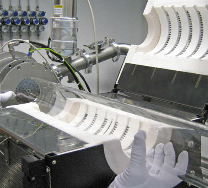
Chemical vapor deposition (CVD) is a well-known method for applying thin coatings to materials. A material is heated, and a chemical reaction creates a thin film of the gas phase on this material. FHR offers special solutions for this type of coating, especially for wires and fibers, e.g. made of carbon or silicon carbide.
CVD coatings require high temperatures of at least 500 °C and a high energy supply. A vacuum generated within the process chamber simplifies the process by reducing the boiling point for the transition of precursor substances into the gas phase and preventing unwanted chemical reactions.
One advantage of the CVD method when compared to the PVD process, for example, is that it can evenly coat complex and three-dimensional surfaces. This makes it possible to create extremely fine structures on semiconductor discs – so-called wafers.
CVD coating requires special starting materials that contain all the necessary components for the desired coating. For example, ammonia and dichlorosilane are used as starting materials for a silicon nitride coating. Tin chloride or tin-organic compounds, as well as oxygen or water vapor, are used for thermal barrier coatings on glass made of tin oxide. Such tin oxide coatings also protect container glass in bottling systems, for example, from damage caused by impacts and other mechanical effects.
In view of the fact that the condition of the substrate surface has an influence on the coating growth, it is possible to grow metals specifically in certain sections of the surface – for example, only in electrically conductive areas, but not in insulating areas – if the process is designed accordingly. These possibilities for selective coating make CVD and PECVD particularly interesting for microelectronics.
Other technologies and coating processes
-
 Sputter Technology
Magnetron Sputtering
Strong magnetic fields enable uniform and high-quality coating formation.
-
 Sputter Technology
Co-sputtering
Production of flexibly adjustable mixed coatings with varying compositions.
-
 Sputter Technology
Confocal Sputtering
Use of up to five different materials in a single chamber to ensure a high degree of flexibility and customized coating composition.
-
 Thin Film Technology
PVD Coating
Vaporization of solid targets in the process chamber – This is used, for example, in the semiconductor industry, the optical industry, or in architecture.
-
 Thin Film Technology
Thermal Evaporation
Suitable for applying materials such as copper, silver, or gold, but also other materials such as silicon dioxide or indium tin oxide.
-
 Thin Film Technology
PECVD Coating
Coating process for coating at low temperatures between 200 °C and 500 °C.
-
 Thin Film Technology
ALD & SALD
ALD can be used to produce uniform, very thin coatings on complex surfaces at low temperatures.
-
 Layer Structuring
Plasma Etching
Plasma etching is used to remove materials from a substrate with extraordinary precision.
-
 Layer Structuring
Reactive Etching
With the possibility of carrying out both isotropic and anisotropic etching, reactive ion etching offers a high degree of flexibility in the structuring of surfaces.
-
 Functional Layers
Optical Coatings
Coatings for the mirroring and anti-reflective coating of optical surfaces.
-
 Functional Layers
Electronic Coatings
Electronic coatings with different properties.
-
 Functional Layers
Antireflective Coatings
Anti-reflective, dielectric coatings for anti-reflective glass surfaces.
-
 Functional Layers
Decorative Coatings
Coatings for finishing materials.
-
 Functional Layers
Tribological Coatings
Coating for achieving a reduction in adhesion and friction, or for abrasion and wear protection.
FHR – The Right Partner at Your Side
Shaping the future together – with reliable and high-quality coating solutions from FHR:
- Industry-leading quality: Our vacuum coating systems are designed for maximum precision and durability.
- Customized solutions: We offer individual solutions for your coating project that meet your specific requirements.
- Innovative methods and technologies: With our many years of experience and expertise in vacuum coating, we continue to set new standards.
- Dedicated customer service: Our experienced team is always available to answer your questions and provide you with support in your projects.
Discover the diverse range of possibilities with our vacuum coating technology, and place your trust in FHR as your reliable partner for outstanding coating solutions. Please feel free to get in touch with us to find out more and realize your projects together.

Your Contact Person
Do you have any questions?
Would you like to discover more about thin film technology or receive general advice on our vacuum coating systems and our coating service? Then feel free to get in touch with us – our team of experts will be happy to answer all your questions.