
Your First Step to the new Product
Are you looking for a suitable coating process? Do you want to first test thin film systems on samples for qualification? Does your company produce in small batches and is looking for a service provider to provide your products with a suitable coating?
Be it a single wafer or a small series: Ask us – we offer you production capacity in our application laboratory on our in-house coating systems, as well as experienced experts who are on hand to provide you with help and advice.

Systems on Site
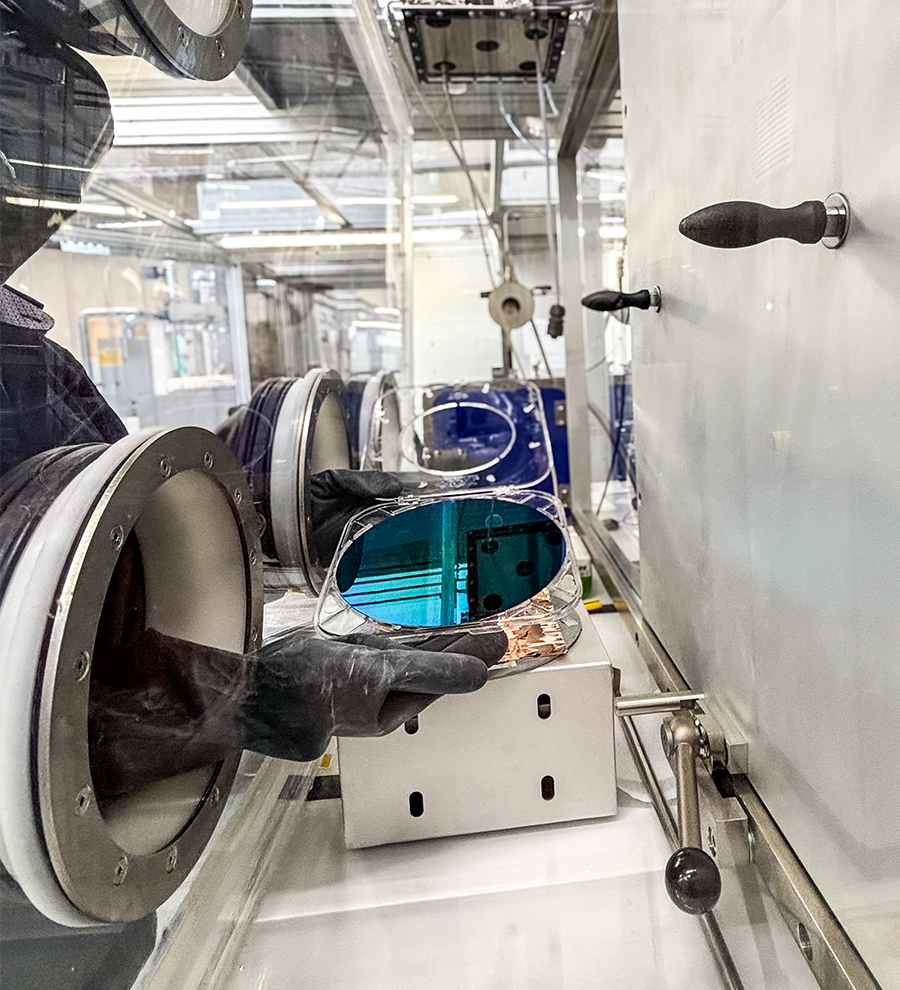
OUR APPLICATION LABORATORY
Our application laboratory comprises a wide variety of system types. Regarding coatings, the suitable system depends on the substrate type and size and the desired separation technologies. With system construction, service, and automation directly in-house, these systems can be customized if required. Please do not hesitate to contact us. We can also test newly developed targets for you directly in the application laboratory at FHR.
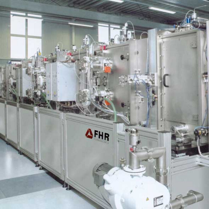
FHR.LINE.400-V
- Substrate size: 360 x 400 mm
- Plasma etching
- Process: Sputtering (DC, MF, RF)
- Material: ceramics, wafers, polymers, metals, glass
We are an all-rounder in pattern coating, from simple metallic coatings to functional AR coatings.
2 x FHR.Line.600-H
- Substrate size: 300 x 300 mm, 500 x 500 mm
- Plasma etching
- Process: Sputtering (DC, MF, RF)
- Material: ceramics, wafers, polymers, metals, glass
The primary area of application is sensor production.
Retrofit or new installation
If the capacities are not sufficient (anymore), we offer you the next step with a retrofit of your existing vacuum coating system or the production of a new one.
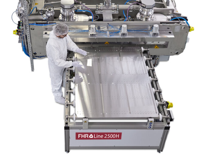
FHR.Line.2500-H
- Substrate size: 2200 x 1400 mm
- Plasma pre-treatment
- Process: Sputtering (DC)
- Material: ceramics, wafers, polymers, metals, glass
FHR.Line.2500-H is mainly used for large substrates and larger quantities.
FHR.Star.300-ALD
- Substrate size: Diameter 300 mm
- Substrate height: ≤10 mm
- Substrate weight: ≤700 g
- Process: Thermal and Plasma ALD
- Material: SiO2, ZnO, TiO2, Al2O3, SnO2, Ta2O5, SiN, AlN, TiN, HfO2, ZrO2, Ta:TiO2, Al:ZnO
- Substrate: ceramics, wafers, polymers, metals, glass
- Process temperature: 80-400°C (depending on material)
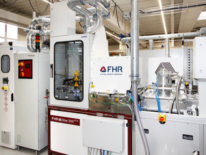
Atomic layer deposition (ALD) is a highly controlled thin-film process based on cyclical, self-limiting chemical reactions. This technology enables the layer-by-layer build-up of ultra-thin films – often in the range of single atomic layers.
Initially developed for the requirements of the semiconductor industry, ALD is now used wherever the highest demands are placed on layer thickness, homogeneity, and conformity. The strength of this technology is particularly evident in complex 3D substrates with high aspect ratios: ALD coats even the finest structures absolutely evenly.
In addition to micro- and nanoelectronics, ALD is widely used in energy technology, sensor technology, and medical technology—for example, in the production of functionalized surfaces or protective coatings. The technology opens up new design possibilities for the development of high-performance, durable, and customized coating systems.
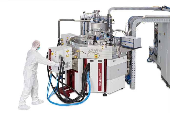
FHR.Star.500-EOSS®
- Substrate size: Diameter 200 mm
- Process: Sputtering in meta mode
- Material: oxides & nitrides
The systems included in our FHR.Star-EOSS® product family are based on customer requirements for a precision sputtering system for the deposition of optical multi-layers that meet the highest demands regarding layer quality and layer thickness homogeneity on predominantly flat substrates. Our precision sputtering systems are suitable for depositing interference-optical coating systems to produce dielectric mirrors and optical filters, such as Bandpass or multiple-notch filters.
FHR.Star.300-EVA
- Substrate size: Diameter max. 300 mm
- Substrate weight: ≤1000 g
- Process: Thermal evaporation
- Material: C60, Ag, Sb, Bi, etc.
- Substrates: Ceramics, wafers, polymers, metals, glass, etc.
- Crucible temperature: max. 1500 °C
- Base pressure: 10-(6-7) mbar
- 2 sources

Thermal evaporation is one of the established methods of physical vapor deposition (PVD) and is used under vacuum conditions. It is characterized by a high deposition rate, which, in combination with comparatively simple process control, offers an economically attractive coating solution.
The process enables the uniform deposition of thin layers on a wide variety of substrate materials – from flexible metal and polymer films to glass and structured silicon. In addition to its easy scalability for large-area applications, thermal evaporation offers a wide range of materials and high process stability.
This process is used in electronics manufacturing, for optical and decorative coatings, in photovoltaics, and in packaging and barrier technology, among other areas. Thermal evaporation thus remains a versatile and proven solution when efficiency, material diversity, and high production speeds are required.
Get in Contact
Do you have any questions?
Regardless of whether sampling or a small series — our team is always happy to support you. Email us or simply give us a call and let our experts be at your service.